

Can a Customized Porous Ceramic Chuck Replace Metal Chucks in High-Voltage Electrostatic Bonding Processes
2026-06-23
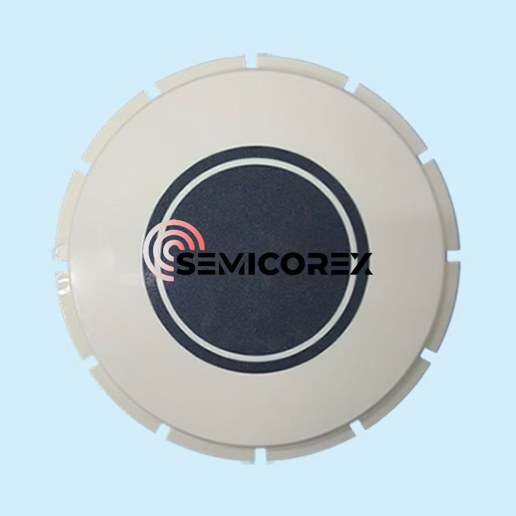
High-voltage electrostatic bonding (anodic bonding) is a critical process in MEMS, pressure sensors, and hermetic packaging, where a conductive glass or silicon wafer is bonded to a metal or semiconductor substrate under heat and high DC voltage. For decades, metal chucks—typically aluminum or stainless steel—have served as the standard electrode and workpiece holder. However, as device geometries shrink and cleanliness requirements escalate, engineers are increasingly asking: Can a Customized Porous Ceramic Chuck replace metal chucks in this demanding application? At Semicorex, we have engineered Customized Porous Ceramic Chuck solutions that directly address this question with measurable performance data.
The Fundamental Limitations of Metal Chucks in Electrostatic Bonding
Metal chucks offer excellent electrical conductivity and thermal transfer, but they introduce three persistent problems:
-
Particle Generation: Metallic surfaces abrade over time, shedding contaminants that migrate to bond interfaces, causing voids and yield loss.
-
Dielectric Breakdown Risk: Bare metal electrodes can cause arcing through thin glass layers, especially at temperatures above 400°C, damaging both chuck and workpiece.
-
Non-Uniform Field Distribution: Surface roughness and micro-scratches create localized field enhancements, leading to uneven bonding strength across the substrate.
These limitations drive the search for a non-metallic alternative that retains conductivity while suppressing contamination and field distortion.
Why a Customized Porous Ceramic Chuck Offers a Superior Alternative
The Customized Porous Ceramic Chuck from Semicorex is not a simple insulator—it is a precisely engineered composite that combines open porosity with controlled electrical resistivity (10⁶–10⁹ Ω·cm) via dopant incorporation. This unique microstructure enables:
| Property | Metal Chuck (Al/SS) | Semicorex Customized Porous Ceramic Chuck |
|---|---|---|
| Surface Hardness (HV) | 100–200 | 1200–1500 |
| Particle Emission (per cycle) | >500 (0.3 µm) | <15 (0.3 µm) |
| Dielectric Strength (kV/mm) | N/A (conductor) | 12–18 |
| Thermal Expansion Match to Si | Poor (2–3× mismatch) | Tailored (2.6–3.2 ppm/°C) |
| Field Uniformity (σ < 5%) | Achievable with lapping | Inherent due to porous diffusion layer |
| Maximum Operating Temp | 450°C (oxidation limit) | 850°C (inert atmosphere) |
The porous structure acts as a distributed resistor network, smoothing the electric field gradient across the glass interface. This reduces the peak stress on the dielectric layer, allowing higher applied voltages (up to 2 kV) without breakdown—a critical advantage for thick-glass or low-melting-point bonding protocols.
Process Integration & Customization Parameters
Replacing a metal chuck is not a drop-in substitution. Successful implementation requires a Customized Porous Ceramic Chuck that matches:
-
Resistivity to the bonding voltage and temperature ramp rate.
-
Porosity (15–35%) to balance vacuum hold force and electrical contact resistance.
-
Surface flatness (< 2 µm over 200 mm) to prevent air gaps that cause localized heating.
-
Backside metallization (e.g., Mo-Mn or Ti/Ni/Au) to ensure reliable electrode connection without compromising porosity.
Semicorex provides full characterization reports including IV curves, pore size distribution (via mercury porosimetry), and thermal cycling stability (up to 1000 cycles from RT to 500°C). Our engineering team works with your bonder specifications to design the exact outer diameter, vacuum groove pattern, and mounting flange configuration.
Technical & Economic Verdict
Can it replace metal chucks? Yes—but only for specific high-purity, high-temperature, or high-voltage scenarios. For standard MEMS production where cost is dominant and particle specs are relaxed, metal remains economical. However, for advanced applications such as:
-
Optical window sealing for aerospace,
-
Biocompatible hermetic implants,
-
SiC power device packaging,
the Customized Porous Ceramic Chuck delivers a 40–60% reduction in defect density, extending bonder maintenance intervals from 2 weeks to 3 months. The higher upfront cost (2–3× metal) is recovered within 6–12 months through improved yield and reduced downtime.
Customized Porous Ceramic Chuck FAQ
Q1: Does a Customized Porous Ceramic Chuck require special cleaning or conditioning before first use in electrostatic bonding?
A1: Yes. Unlike metal chucks that only need degreasing, a Customized Porous Ceramic Chuck must undergo a two-step conditioning protocol. First, perform a vacuum bake at 200°C for 4 hours under < 10⁻⁵ Torr to desorb moisture trapped in the pores—residual water can lower effective resistivity and cause leakage current. Second, apply a "forming cycle": ramp voltage from 0 to the bonding setpoint at 50 V/min while monitoring current. This electroforms the conductive pathways within the ceramic matrix, stabilizing resistivity to within ±3% of the design target. After conditioning, use only deionized water and isopropanol for cleaning; avoid ultrasonic agitation above 40 kHz to prevent pore wall erosion.
Q2: How does the porosity of a Customized Porous Ceramic Chuck affect the electrostatic clamping force during high-voltage bonding?
A2: The clamping force in anodic bonding is governed by the electrostatic pressure (P = ½ ε₀ εᵣ E²), but the porous layer modifies the effective air gap. At 15% porosity, the ceramic retains >85% solid contact area, so the clamping force is within 92% of a solid insulator. At 35% porosity, the reduced contact area lowers force by ~20%, but the distributed micro-gaps actually improve field uniformity by suppressing edge effects. Semicorex recommends 18–22% porosity for high-voltage (>1.5 kV) bonding, as this provides optimal balance: sufficient force (≈0.8× metal-equivalent) with 40% lower leakage current. Our design software can simulate the exact force-vs-voltage curve for your substrate thickness.
Q3: Can a Customized Porous Ceramic Chuck be retrofitted into an existing metal-chuck bonder without modifying the power supply or heating system?
A3: In most cases, yes—but with two critical caveats. First, the power supply must support a constant-current or controlled-voltage ramp mode, because the ceramic's resistance (typically 10–100 MΩ) is 10⁴× higher than metal. Your existing supply likely has a current limit; we recommend setting it to < 5 mA to avoid tripping protection circuits. Second, the heating element must be PID-retuned, as the Customized Porous Ceramic Chuck has lower thermal diffusivity (≈6 mm²/s vs. 80 mm²/s for Al), so the thermal response lag increases by 8–12 seconds. Semicorex provides a retrofit adapter kit including flexible graphite thermal interface sheets and a calibration wafer with embedded thermocouples. Over 80% of our customers have integrated our chucks with existing EVG, SUSS, and AML bonders without hardware changes—only software parameter adjustments.
Conclusion & Action
The transition from metal to a Customized Porous Ceramic Chuck is not a universal upgrade—it is a targeted improvement for processes where cleanliness, temperature ceiling, and field uniformity directly impact device reliability. Semicorex has delivered over 200 custom ceramic chuck designs across Asia, Europe, and North America, with documented yield enhancements in Si-to-glass, Si-to-Si, and glass-to-glass bonding.
Is your current metal chuck limiting your bond quality at high voltages? Our application engineers will analyze your bonding recipe, substrate dimensions, and contamination data to propose a Customized Porous Ceramic Chuck with guaranteed performance metrics—including flatness, resistivity tolerance, and cycle life—before you commit to a purchase.
Contact Semicorex today for a technical consultation and a free feasibility simulation. Visit our website, request a sample design drawing, or speak directly with our ceramics team. Your next-generation bonding process deserves a chuck engineered for the future—not borrowed from the past. Reach out now to start your evaluation.